Projects
Ongoing Projects
- TBD
Completed Projects “Click On the Links for presentation files”
- FPGA Based Real-Time Image Processing Photo Booth, 2025.09.08 - 2025.09.30, Final Project, 대한상공회의소 서울기술교육센터
- RV32I 기반 RISC-V FPGA MCU 및 APB 버스 설계 검증, 2025.08.06 - 2025.09.05, SoC System on a Chip , 대한상공회의소 서울기술교육센터
- 512 – Point radix FFT 설계 및 검증, 2025.07.15 - 2025.08.05, ASIC Front End Design, 대한상공회의소 서울기술교육센터
- YOLOv5 기반 공항 조류(Bird Strike) 탐지·경보 시스템, 2025.06.23 - 2025.07.11, AI and Algorithm, 대한상공회의소 서울기술교육센터
- Stopwatch and Timer, 2025.05 - 2025.06, System Semiconductor Design, 대한상공회의소 서울기술교육센터
- DOOM : C Slayer, 2025.03 - 2025.05, ARM System Programming, 대한상공회의소 서울기술교육센터
- Fast Fourier Transform (FFT) Implementation with Software and Hardware, 2023.09 - 2024.06, Capstone Project, KwangWoon University
- UART Transmitter and Reciever IP Development, 2023.09 - 2023.12, 광운튜터링, KwangWoon University
- Understanding Data Conversion by implementing Delta Sigma and Flash Analog to Digital Convertors, 2023.09 - 2023.12, 전자회로실험2 Term Project, KwangWoon University
- Analog Computer, 2022.03 - 2022.06, 전자회로실험1 Term Project, KwangWoon University
- Development of a Simple Graphics Card and Sound Card, using DE1 - SoC FPGA Board, 2019.09 - 2019.12, 기초전자실험 Term Project, KwangWoon University
- Development of a Calculator using C++ and MFC, 2019.03 - 2019.06, 소프트웨어설계 Term Project, KwangWoon University
- LASER Communication, 2019.03 - 2019.06, 기초전자실험 Term Project, KwangWoon University
- Handicapped and IoT (Canes for the Challenged), 2018.10 - 2018.12, 공학설계과제, KwangWoon University
Contest
Project Details
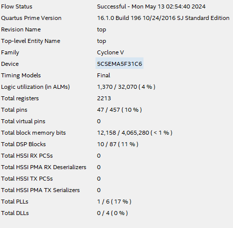
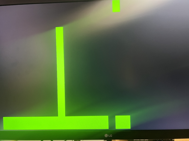
FPGA Based Real-Time Image Processing Photo Booth
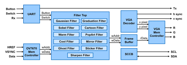
FPGA Based Real-Time Image Processing Photo Booth Block Diagram
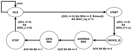
OV7670 Camera Interface FSM
-
Project Name: FPGA Based Real-Time Image Processing Photo Booth
-
Main Function: Real-time image processing photo booth implemented on FPGA.
-
Detail: Developed an FPGA-based photo booth capable of real-time image processing using OV7670 camera input. Designed and verified multiple filters (Mirror, Gaussian, Ghost, Graduation) and implemented a camera interface and UART/button control to switch between effects. Added features to save images and select different filters dynamically.
RV32I RISC-V FPGA MCU & APB Bus Design Verification
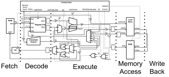
RV32I RISC-V MCU Block Diagram
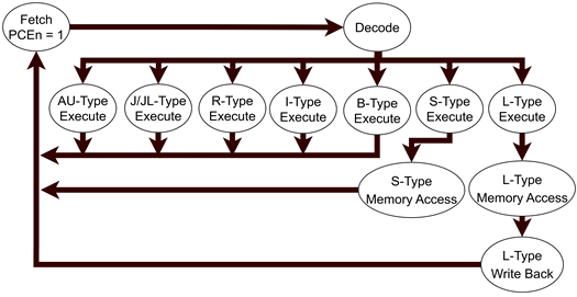
RV32I RISC-V MCU FSM
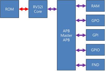
APB Bus Block Diagram
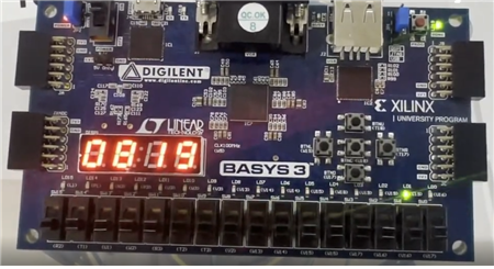
Counter and LED C Program Working
-
Project Name: RV32I-based RISC-V FPGA MCU & APB Bus Design Verification
-
Main Function: Designed and verified an RV32I RISC-V CPU with AMBA-APB bus on FPGA.
-
Detail: Implemented a single-cycle and multi-cycle RV32I CPU in SystemVerilog. Created AMBA-APB peripherals (GPIO, FND) and wrote RV32I Assembly test programs. Verified integration and functionality with Verdi and Vivado, demonstrating SoC-level peripheral control on FPGA.
512–Point radix FFT Design & Verification
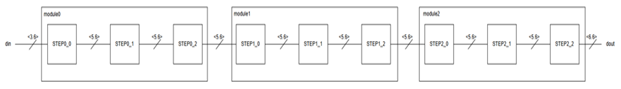
512–Point radix FFT Design Block Diagram
FFT FPGA Block Diagram
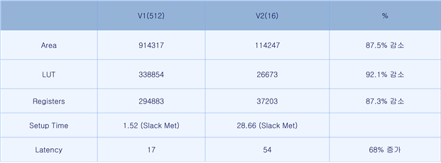
FFT FPGA Block Resource Reduced
-
Project Name: 512–Point radix FFT Design & Verification
-
Main Function: Designed and verified a 512-point radix FFT IP core.
-
Detail: Used SystemVerilog to implement a 512-point FFT pipeline for high-speed signal processing. Performed simulation and verification with Synopsys Verdi and Xilinx Vivado. Acted as team leader for module0 and top-level integration, verifying timing and correctness using generated test vectors.
YOLOv5 Bird Strike Detection & Alert System
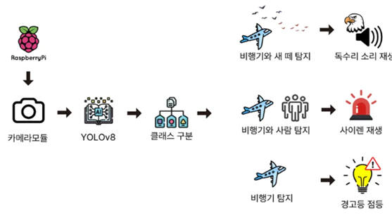
YOLOv5 Bird Strike Detection & Alert System Block Diagram
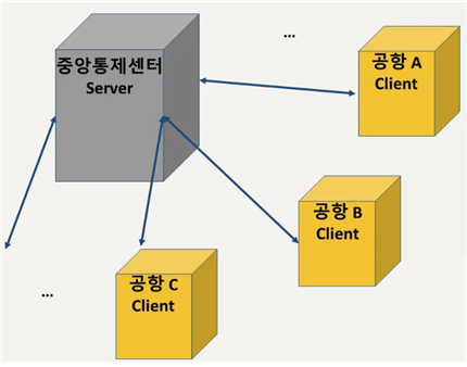
YOLOv5 Bird Strike Detection & Alert System Network Diagram
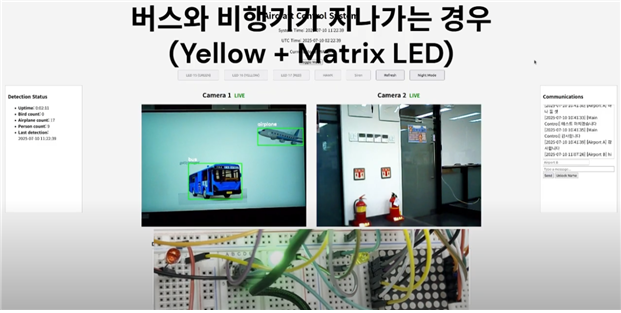
YOLOv5 Bird Strike Detection & Alert System Demo
-
Project Name: YOLOv5 Bird Strike Detection & Alert System
-
Main Function: Developed an AI-based bird strike detection and alert system using YOLOv5.
-
Detail: Built a Raspberry Pi + camera system running Python and YOLOv5 to detect birds in real time near airports. Implemented server-client communication to send alerts and display results. Verified detection accuracy with various video sources.
Smart Clock
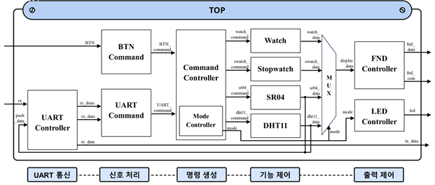
Smart Clock Block Diagram
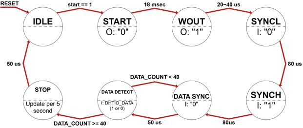
Sensor DHT11 FSM
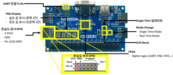
Smart Clock Connection
-
Project Name: Stopwatch and Timer on FPGA
-
Main Function: Implemented a Watch-Stopwatch/Timer system using Xilinx FPGA and Vivado.
-
Detail: Designed a Watch-Stopwatch with UART, ultrasonic/temperature sensors, and integrated them into a smart watch system on FPGA. Verified timing accuracy, sensor interfacing, and UART communication.
System Programming on a ARM Cortex-M3 Development Board

Game Process and File Structure

UART Commands for the game (God Mode)
-
Project Name: DOOM : C Slayer
-
Main Function: 2-D Game made with C programming on a ARM Cortex-M3 Development Board.
-
Detail: When you first turn on the device, the game will ask to press switch 0 for to start the game. You then briefly read the instrucions and again press switch 0 to selec the difficulty of the game. You can select the difficulty by entering the numbers 1, 2 and 3 respectively EASY, NORMAL and HARD via UART on the serial command line. The game is consisted with 5 stages and addition with the boss stage. The objective of the game is to fight all enemy mobs and the C boss at the end to conquer the C Programming language. If you win all 6 stages you win the game. There are 3 types of mobs, the normal ememy with 2 HP, fast type enemy with 1 hp and the slow but heavy tank mob with 4 hp. By every 10 points you can use a perk where 5 shots could be fired on all 4 sides simultaneously.
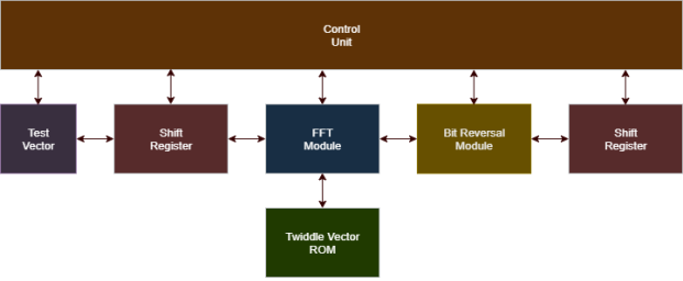
Fast Fourier Transform (FFT) Implementation with Software and Hardware
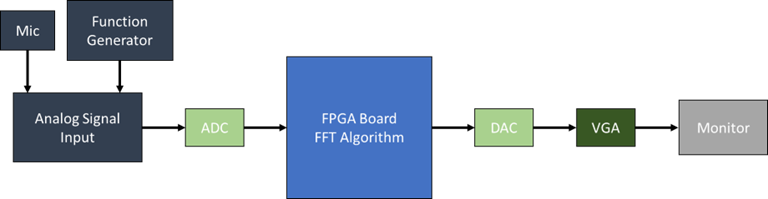
Spectrum Analyzer IP Development Block Diagram
Top Sysnthesis
VGA Memory Mapping
Spectrum Analyzer Under Test! (4Vp-p Sine wave @100Khz)
-
Project Name: Fast Fourier Transform (FFT) Implementation with Software and Hardware
-
Main Function: An Spectrum Analyzer using FPGA SoC Board.
-
Detail: We have made a very simple spectrum analyzer using the DE1-SoC Board. This project starts from sampling signals from the function generator. The signal is sampled using the LTC2308 chip on the board. We can sample up to 250kHz(Sampling Rate: 500kHz). The digital signal is then processed through the FFT Module. This module will input real values(Constraints :No modulated signals input) and will return a magnitude and frequency. This information will be printed via VGA Memory, which is controlled by the VGA Controller. The controller will case each magnitude and freqeuncy to a given slot and will update the screen by page (640x480 @60hz Display).
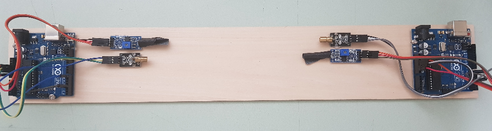
UART Transmitter and Reciever IP Development for Arduino and FPGA Interface
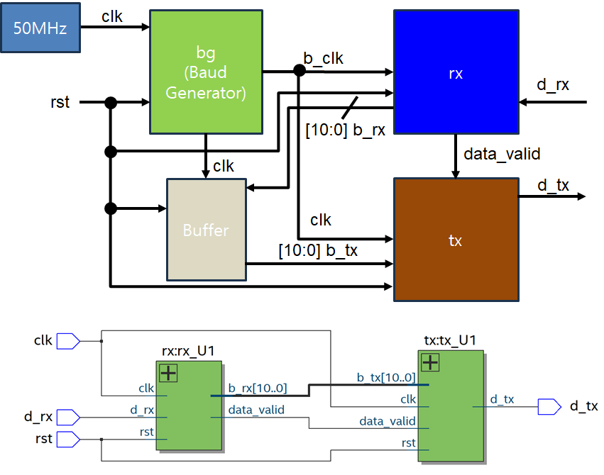
UART Transmitter and Reciever IP Block Diagram

UART Transmitter and Reciever IP TOP file simulation Result
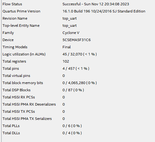
UART Transmitter and Reciever IP Development Summary of Synthesis
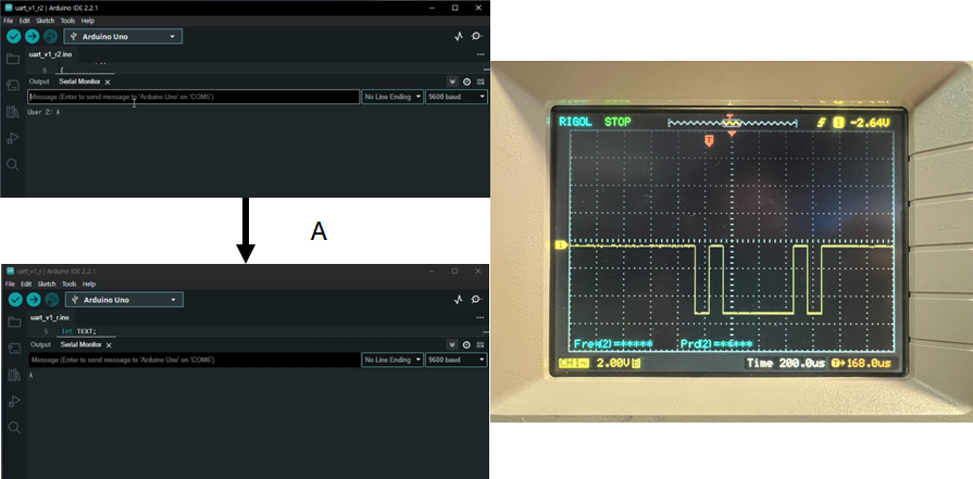
UART Transmitter and Reciever IP Development Oscilloscope Trigger Result
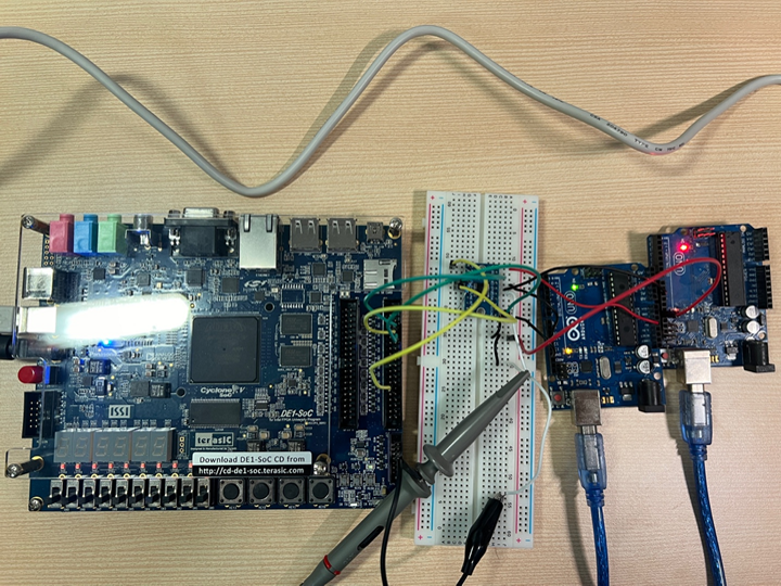
Integration of the entire project
-
Project Name: UART Transmitter and Reciever IP Development for Arduino and FPGA Interface
-
Main Function: An UART communication interface between FPGA and Arduino.
-
Detail: We have designed a UART communication interface for FPGA and Arduino interface. Before designing the interface we must first understand the proctocol from the arduino side. We make a simple chating program and use an oscilloscope to see the protocol. Then we develop the IP from reciever to Transmitter step by step. After numerous testbenches we integrate the system into a top file, synthesis and again test whether the UART is working well by using a oscilloscope.However we must note that since the voltage system is different between Arduino(5V) and FPGA(3.3V) a voltage shifter is needed.
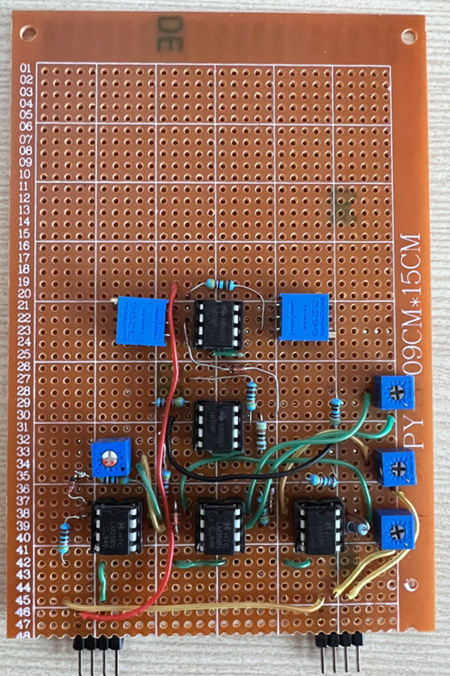
Understanding Data Conversion by implementing Delta Sigma and Flash Analog to Digital Convertors
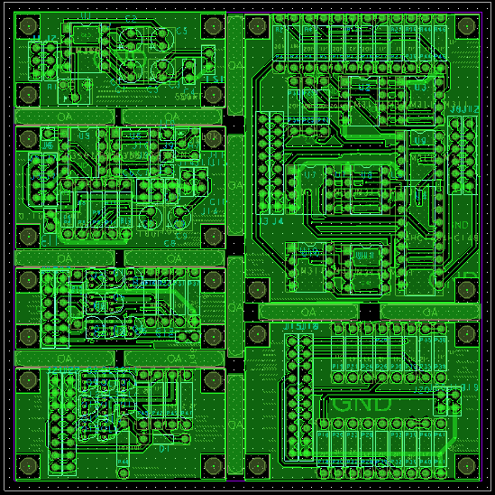
Flash ADC, DAC, Operational Amplifier, Comparator, Pre-Amplifier, Audio Amplifier PCB Artwork
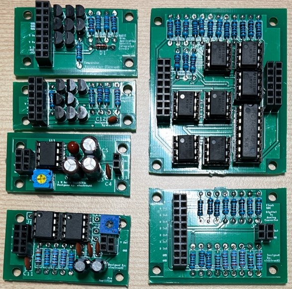
Flash ADC, DAC, Operational Amplifier, Comparator, Pre-Amplifier, Audio Amplifier PCB Artwork Final Result
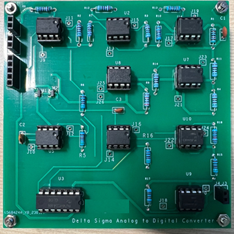
Delta Sigma ADC Final Result
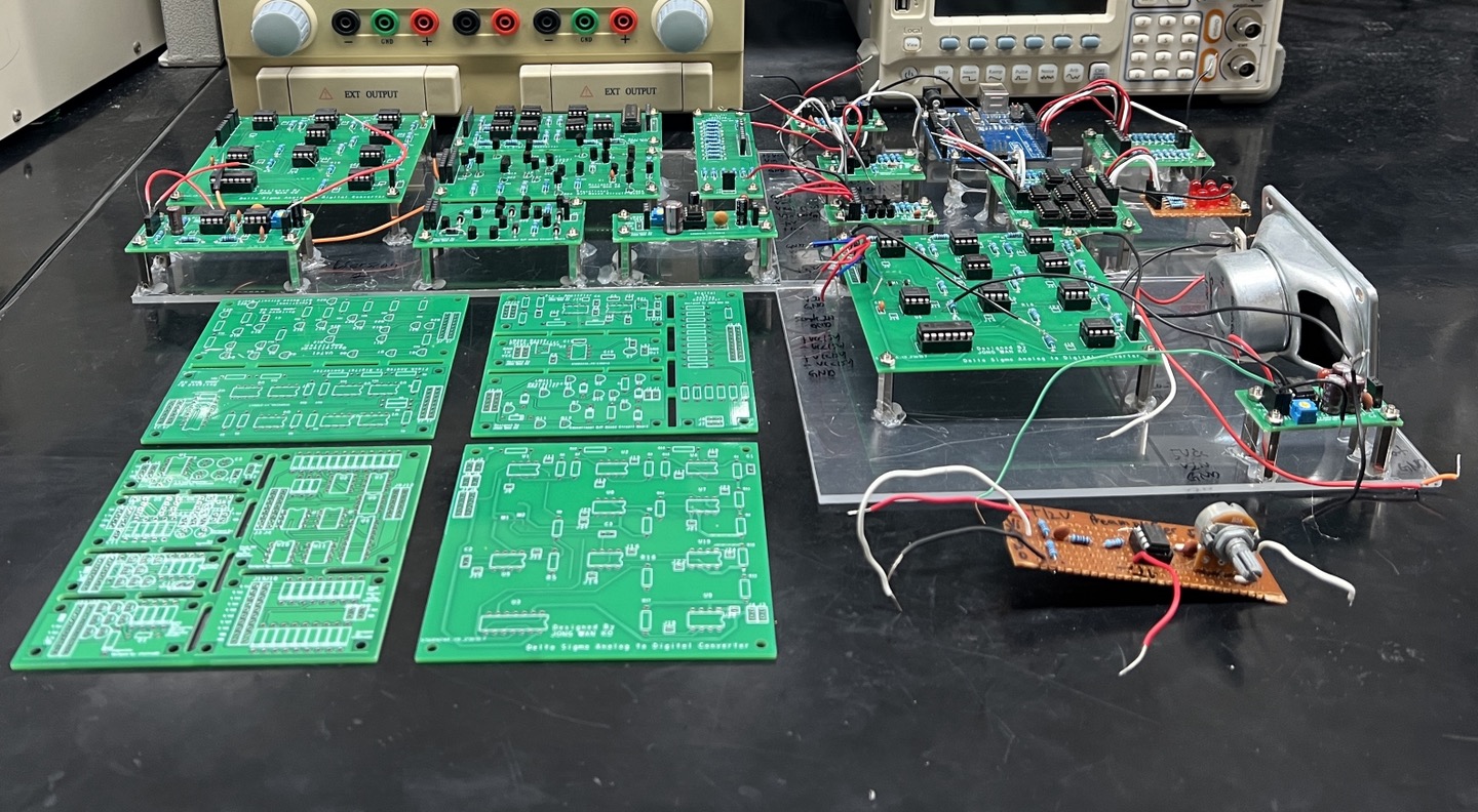
Final Result of the entire project
-
Project Name: Understanding Data Conversion by implementing Delta Sigma and Flash Analog to Digital Convertors
-
Main Function: By designing Operational Amplifiers, Comparators, ADC and DAC we understand the fundamentals of data conversion and basic circuit design.
-
Detail: We have designed a Operational Ampilifer and a Comparator using discrete components to understand the underlying concepts of circuit design. Also we have implemented a flash ADC and a Delta Sigma ADC to understand how data is converted for future reference. We have also covered DAC to fully understand how data is converted from digital to analog form. In this process we have also experimented the use of commercial grade ADC and DAC via sound card on computers, which are excellent examples.
Analog Computer
Multiplication Module
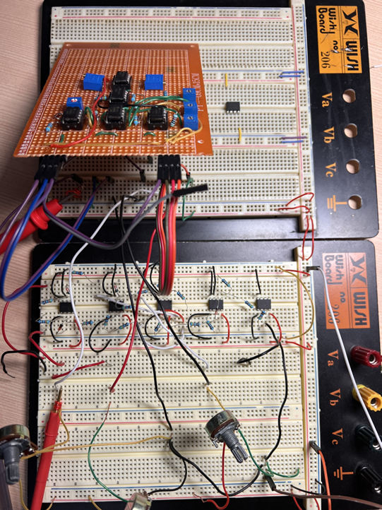
Multiplication Module Under Test
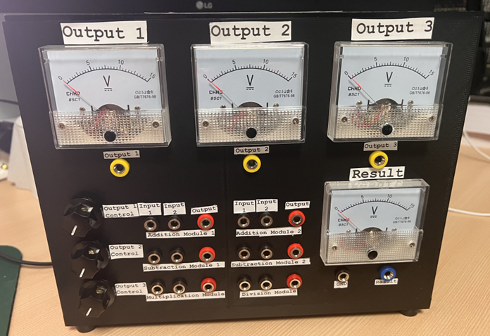
Analog Computer Final Product
-
Project Name: Analog Computer
-
Main Function: Operates Arithmetic operations using only analog circuits.
-
Detail: This device is designed to operate addition, subtraction, multiplication and division. The operation can withstand up to 12 Volts. This project was done to understand the basics of Operational amplifiers and how computation was done before the digital age emerged.
Development of a Simple Graphics Card and Sound Card, using DE1 - SoC FPGA Board
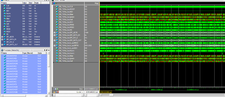
System Simulation
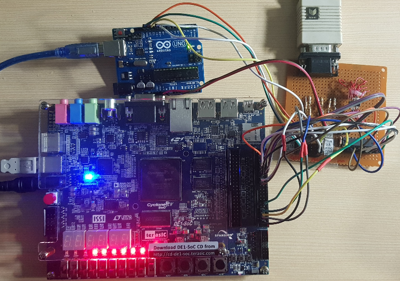
System Integration Test
Image Test, MAGIC!
-
Project Name: Making a Simple Graphic Card & a Simple Sound Card
-
Main Function: Graphic Card Part (electron65 part) A digital signal from the Arduino Uno is sent throught the DE1-SoC FPGA Board. In the process of being sent, it is sent by SPI protocol. From the inside of the FPGA board, the signal is set to coordinate with a specific timmings(Horizontal, Vertical timming). The digital signal is then stored in the DPRAM. In the meantime the data from the DPRAM is transfered through the DAC(Digitial to Analog Converter), changing the signal from digital to analog. From there the data goes through the VGA cable. The data we made from the Arduino Uno finally prints on the monitor.
Detail: Outputs signals through a monitor and a speaker from an Arduino Uno or an SD card.
LASER Communication
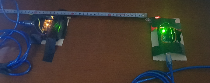
Laser Communication Test
Laser Communication Final Product
Laser Communication!
-
Project Name: Laser Communication
-
Main function: Communicates using laser pulses.
-
Detail: A user will type a character or a string. The data is converted into binary numbers. Each binary number is matched to “On” or “Off” (ex. 1 - ON, 0 - OFF). The laser module then blinks at each data. On the other side of the laser would be a Photolight sensor. The senser takes the light being sent. The “On” and “Off” is then again matched to each binary number. Finally the binary number is converted back and printed on the screen.
Handicapped and IoT (Canes for the Challenged)
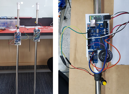
Cane Device
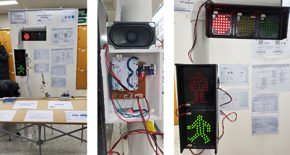
Cane Device Final Product
-
Project Name: Handicapped & IoT Technology
-
Main Function: Helps people who have trouble seeing or are blinded, find there way anywhere and anytime by directing them through sound signals.
-
Detail: Bluetooth modules that are installed in everyday items or facilities such as phones, hospitals or even traffiic lights can communicate with the challenged, especially through the cane. The user first makes a interaction (ex. taps the button 2 times) with the cane. The corresponding reponse from the challenged will be sent to the current connected device (ex. traffic light). The device will then respond with an answer sent back to the cane. The respond then will be read in voice, giving a possibly current location, direction or other cases which correspond to the users demand.